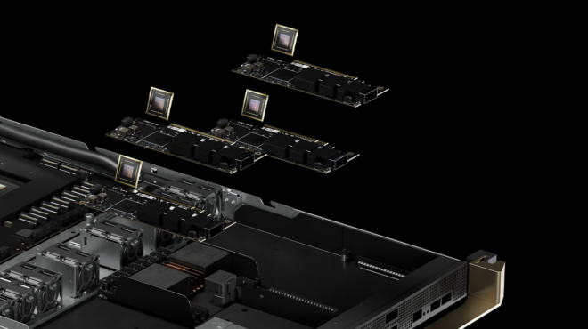
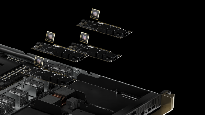
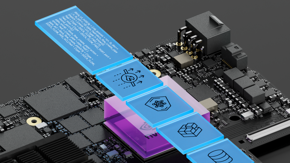
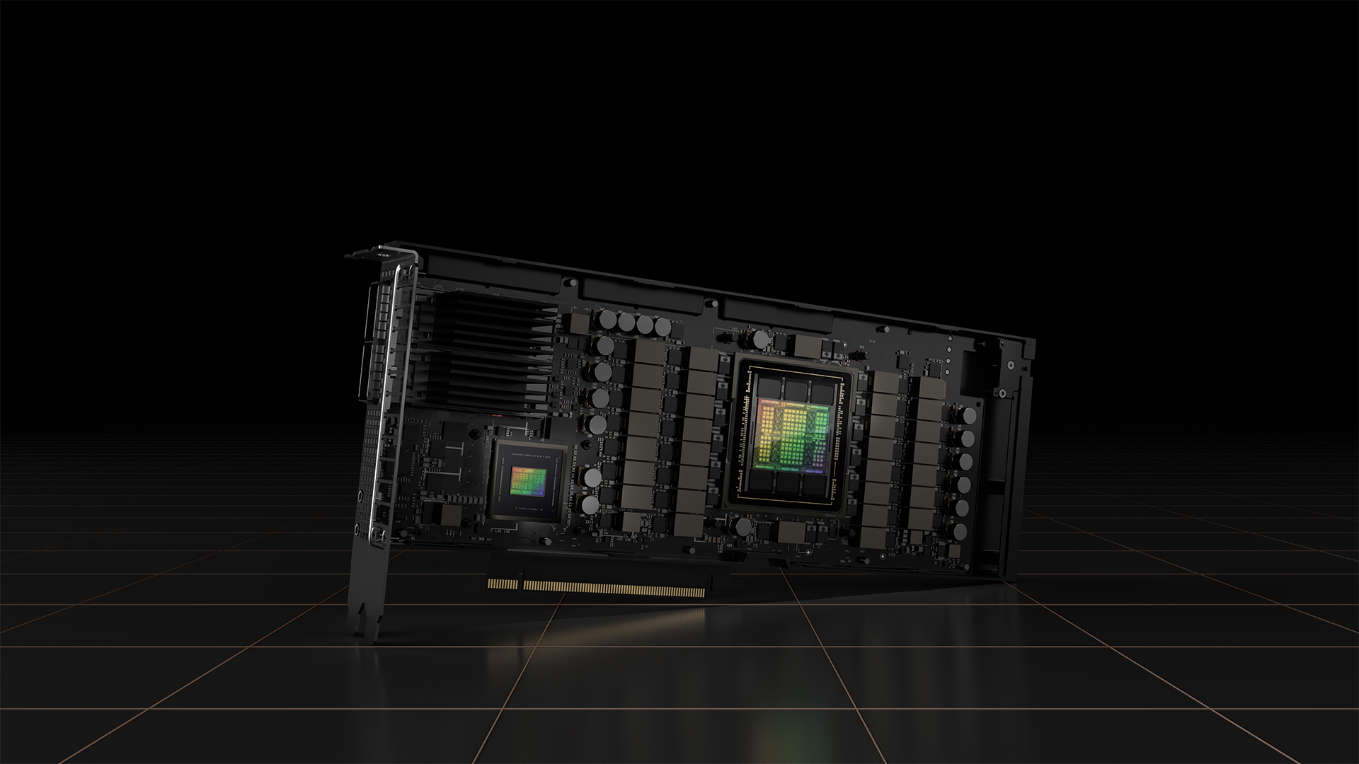
NVIDIA is breaking new ground by integrating silicon photonics directly with its NVIDIA Quantum and NVIDIA Spectrum switch ICs. At GTC 2025, we announced the world’s most advanced Silicon Photonics Switch systems, powered by cutting-edge 200G SerDes technology. This innovation, known as co-packaged silicon photonics, delivers significant benefits such as 3.5x lower power consumption, reduced latency, and dramatically improved network resiliency over traditional pluggable optical transceivers—key factors for accelerating large-scale AI model development and inference.
What is co-packaged silicon photonics?
Co-packaged silicon photonics is an evolution in hardware integration. By placing silicon photonics optical transceivers directly on the same package as the switch ICs, NVIDIA can do the following:
- Reduce power consumption: Co-packaged Silicon Photonics slash power consumption by 3.5x compared to traditional pluggable transceivers. By eliminating bulky external DSPs and reducing the signal path from inches to millimeters, this breakthrough technology dramatically boosts power efficiency. The result: denser, more sustainable AI infrastructure that drives faster insights and scales to meet the demands of the next generation of agentic AI.
- Reduce component count: Fewer parts mean simpler manufacturing and fewer points of failure. Integrating optical components directly on the package reduces the complexity of sourcing, assembling, and testing numerous tiny parts—a common challenge with traditional transceiver systems.
- Enhance performance: With optics integrated, the connection between the switch ASIC and optical transceivers are designed, assembled, and tested at the IC packaging level, eliminating sources of signal degradation and removing the need for separate digital signal processors (DSPs) that traditionally introduce latency and consume extra power.
- Streamline data center operations: Simplified construction leads to faster deployment and easier maintenance.
Key advantages of NVIDIA silicon photonics-based switches
Here are the standout advantages that NVIDIA photonics networking switches brings to modern data centers.
Lower power consumption
Traditional transceivers use DSPs that add significant power draw. For instance, a 1.6 Tbps transceiver might use around 30 watts, with the DSP consuming more than half of that.
By taking advantage of NVIDIA integrated silicon photonics, the power savings over traditional transceivers for AI datacenters translates to 3.5x for massive long-term savings.
Increased network uptime and reliability
When a traditional transceiver fails, it can take hours of manual intervention to troubleshoot and repair. In contrast, co-packaged silicon photonics uses a simpler design with fewer components, significantly reducing the likelihood of transceiver failures. This integrated design minimizes AI data center downtime, enhances network resiliency, and ensures that the network remains fully operational—critical for uninterrupted AI training and inference.
Lower latency and improved signal integrity
NVIDIA Silicon Photonics integrates optical signaling directly into the switch IC package, improving signal integrity by reducing the number of components and dramatically shortening the signal path. In traditional transceiver-based switches, signals travel 14-16 inches over printed circuit boards or copper wires, increasing the risk of signal corruption. With silicon photonics, the signal path is less than half an inch, greatly reducing this risk.
Transceiver-based switches also rely on DSPs (digital signal processors) to clean up signal corruption, which adds significant latency. By integrating silicon photonics directly into the switch IC, this extra processing is eliminated, resulting in lower latency and more efficient networking—critical for high-speed AI workloads and modern data center performance.
Faster deployment
With co-packaged silicon photonics, system installation becomes a straightforward “unbox and install” process enabling 1.3x faster deployment, compared with similar systems deployed with pluggable transceivers.
Easy field serviceability
Should a failure occur, the design places the most failure-prone components—the lasers—on easily accessible external laser source (ELS) pluggable OSFP modules on the switch front panel, facilitating quick diagnosis and easy replacement.
The Innovation Story: Collaboration and breakthroughs
The development of co-packaged silicon photonics has been a multi-year effort—four years in the making—with contributions from hundreds of patents and collaboration with our ecosystem innovation partners.
Through collaborations dating back to 2016, NVIDIA has continuously pushed the technology boundaries of what’s possible and established some of the most stringent industry technical specifications needed for AI networking.
Silicon photonics CPO fabrication, packaging, and test
- TSMC: The TSMC silicon photonics Compact Universal Photonic Engine (COUPE) process integrates electronic integrated circuits (EIC) with silicon photonic integrated circuits (PIC) using the 3D chip-on-wafer and chip-stacking packaging technologies.
- SPIL: SPIL is well-known for packaging complex integrated assemblies including wafer bumping, wafer sort, assembly, and testing for the NVIDIA CPO multi-chip module.?
ELS lasers and subassemblies
- Lumentum, Sumitomo, and Coherent: These vendors provide ELS assembly, optical alignment, and test with the silicon photonics engine.
Optical fiber, connectors, and micro-optics
- Browave, Corning, Senko, TFC Communication, and Coherent: Industry experts with optical connectors and fiber assemblies for linking the ELS lasers with polarization, maintaining fibers into the silicon photonics engine, and data output to the front panel.
Switch packaging
- Foxconn and Fabrinet: These partners provide expertise in system-level CPO assembly and testing, as well as in integrating switch-CPO assemblies and sub-assemblies into the switch system chassis.
Conclusion
NVIDIA’s silicon photonics-based network switching marks a groundbreaking shift in data center networking. By integrating optical transceivers directly with switch ICs, this innovation delivers 3.5x lower power consumption, minimal latency, and unprecedented network resiliency—all critical for powering next-generation AI applications. With faster deployment, simplified design, and enhanced uptime, NVIDIA is not just setting a new industry standard; it’s redefining the future of high-speed, sustainable, and scalable data center infrastructure. This is the dawn of a new era where efficiency meets performance, accelerating AI breakthroughs and reshaping the data center landscape for generations to come.
Stay tuned for more insights into the technologies driving tomorrow’s computing advancements!
Learn more about NVIDIA Silicon Photonics.
